PCB manufacturing · Guilin production base · Shenzhen service officesales@hxlfab.com

Custom PCB manufacturing

Engineering-led PCB manufacturing

HXLFAB supports hardware teams from prototype and NPI through controlled volume production. Every RFQ is reviewed for stack-up, material, impedance, via structure, test coverage and manufacturing risk before commercial confirmation.

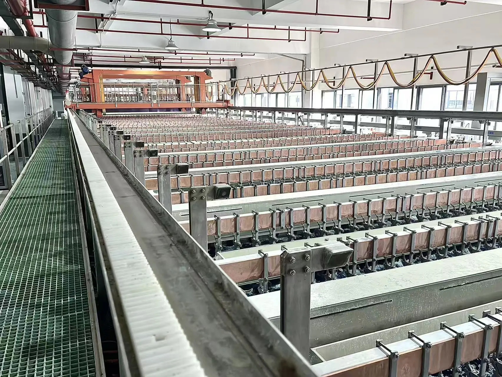
Automated PCB production equipment inside the HXLFAB Guilin factory
Controlled production at the Guilin base
1–30Layer count
3/3 milMinimum trace / space
0.10 mmMinimum laser via
8 ozOuter-layer copper capability

Engineering approach

A manufacturing partner for complex rigid PCBs

PCB sourcing works best when fabrication limits are discussed before release, not after a production hold. HXLFAB combines CAM preparation, material review, automated processing, plating, drilling, inspection and electrical testing within an engineering-led workflow.

Programs can be routed for standard rigid multilayer production or advanced review for HDI, high-frequency, mixed-material, fine-line, heavy-copper and controlled-impedance requirements. Capability values remain subject to the final design, selected laminate and order volume.

What we review before quoting

  • Gerber or ODB++ completeness and fabrication notes
  • Board outline, stack-up, copper distribution and finished thickness
  • Minimum trace, spacing, annular ring and finished-hole requirements
  • Material system, surface finish, impedance and via construction
  • Electrical test, inspection, marking, packaging and compliance requirements

Manufacturing envelope

Capabilities for quotation planning

These values describe the available manufacturing envelope. Final capability, lead time and price are confirmed after review of the actual production data, construction, material and quantity.

Board constructionRigid PCB fabrication from 1 to 30 layers
Feature capabilityDown to 3/3 mil trace and space, subject to design review
Hole and via capability0.15 mm minimum mechanical drill and 0.10 mm minimum laser via
MaterialsTG135 / TG150 / TG170 FR-4, halogen-free, CAF-resistant, PTFE and mixed material systems
CopperUp to 4 oz inner-layer and 8 oz outer-layer capability, subject to review
Panel and thicknessUp to 850 × 520 mm panel; 0.15–7.0 mm finished thickness
Quality controlsAOI, electrical test, impedance measurement, microsection analysis and final inspection

From RFQ to release

A controlled engineering workflow

01 / DATA REVIEW

Check the fabrication package

Gerber or ODB++, drill data, drawings, stack-up and requirements are checked for completeness.

02 / DFM & ROUTING

Confirm the process route

Engineering evaluates materials, features, via construction, test coverage and manufacturing risk.

03 / QUOTE & RELEASE

Issue confirmed terms

Price and lead time are confirmed after the technical route and commercial inputs are aligned.

Applications

Where this capability is used

Communications

Multilayer and RF boards for network and communications equipment.

Industrial control

Reliable fabrication for controls, drives, sensing and automation hardware.

Automotive electronics

Engineering review and controlled production for qualified automotive programs.

Medical equipment

Traceable build documentation and test planning for medical hardware.

AI & computing

Fine-feature multilayer and impedance-controlled boards for compute platforms.

New energy

Power, control and monitoring boards including heavy-copper requirements.

Frequently asked questions

Before you request a quote

Can HXLFAB support both prototypes and volume production?

Yes. Programs can begin with prototype or NPI quantities and transition to controlled volume production after engineering and quality requirements are confirmed.

Do you provide an instant online PCB price?

No. HXLFAB provides an engineer-confirmed quotation after reviewing the production files, construction and quantity. This avoids a misleading price for designs that require special materials or processes.

What should I upload for a quotation?

A compressed Gerber or ODB++ package is preferred. Include drill files, fabrication notes, stack-up, impedance requirements, quantity and any material or certification requirements.

Are uploaded design files public?

No. Files submitted through the RFQ form are stored in private, access-controlled storage and are scheduled for automatic deletion after 60 days.

Ready to review your PCB build?

Upload Gerber files ↗