PCB manufacturing · Guilin production base · Shenzhen service officesales@hxlfab.com

4–30 layer PCB fabrication

Multilayer PCB manufacturer

Build dense, reliable multilayer boards with stack-up, material, impedance and via requirements reviewed before production. HXLFAB supports prototypes, NPI, pilot builds and volume programs up to 30 layers.

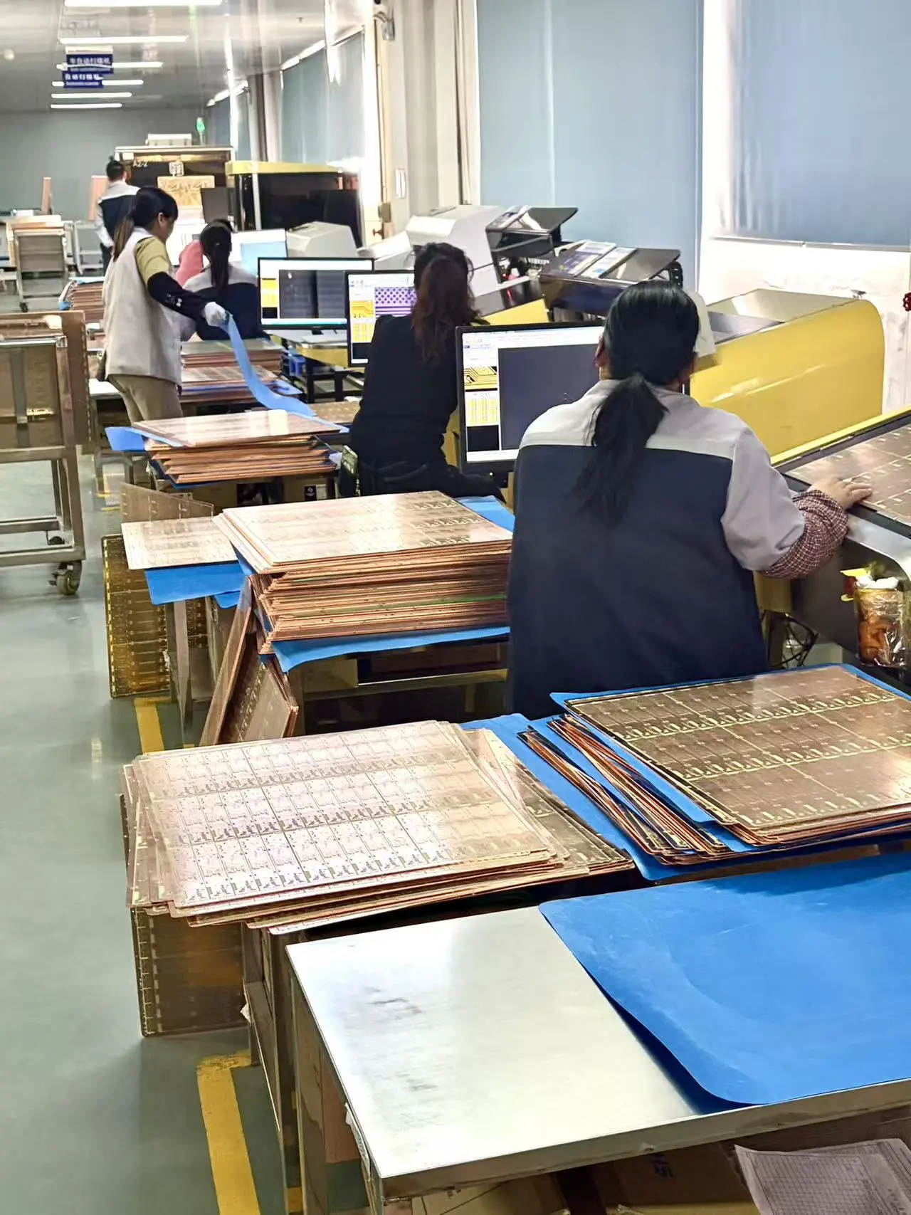
HXLFAB CAM engineers reviewing multilayer PCB production data
CAM and stack-up preparation
4–30Multilayer construction
3/3 milMinimum trace / space
0.15 mmMinimum mechanical drill
0.15–7.0 mmFinished thickness range

Engineering approach

Stack-up discipline before production release

Multilayer PCB performance depends on more than layer count. Copper distribution, dielectric selection, finished thickness, drill aspect ratio, registration and impedance targets must work together as a manufacturable construction.

HXLFAB reviews the supplied stack-up and can flag conflicts among trace geometry, via structure, material availability and finished-board requirements. The confirmed fabrication package becomes the basis for CAM preparation, process routing, inspection and electrical testing.

Best suited for

  • Dense digital and mixed-signal boards
  • Communications, industrial and computing platforms
  • Controlled-impedance layer structures
  • Fine-line routing down to 3/3 mil where the design permits
  • Prototype-to-volume programs requiring consistent construction

Manufacturing envelope

Capabilities for quotation planning

These values describe the available manufacturing envelope. Final capability, lead time and price are confirmed after review of the actual production data, construction, material and quantity.

Layer count4–30 layers
Minimum trace / space3/3 mil subject to design, copper weight and yield review
Minimum mechanical drill0.15 mm
Finished thickness0.15–7.0 mm
Base materialsFR-4 TG135 / TG150 / TG170, halogen-free and CAF-resistant options
Surface finishesLead-free HASL, ENIG, OSP, immersion tin, immersion silver and hard gold subject to specification
TestingAOI plus flying-probe, fixture or four-wire electrical testing as required

From RFQ to release

A controlled engineering workflow

01 / DATA REVIEW

Check the fabrication package

Gerber or ODB++, drill data, drawings, stack-up and requirements are checked for completeness.

02 / DFM & ROUTING

Confirm the process route

Engineering evaluates materials, features, via construction, test coverage and manufacturing risk.

03 / QUOTE & RELEASE

Issue confirmed terms

Price and lead time are confirmed after the technical route and commercial inputs are aligned.

Applications

Where this capability is used

Network hardware

Routers, switches, gateways and communications infrastructure.

Industrial electronics

Controllers, instrumentation, motion and factory automation.

High-end computing

Dense interconnect for servers, accelerators and embedded compute.

Medical systems

Diagnostic, monitoring and control electronics.

Automotive modules

Qualified multilayer programs for automotive electronics.

Energy systems

Control, monitoring and power-management electronics.

Frequently asked questions

Before you request a quote

What files are needed for a multilayer PCB quote?

Upload Gerber or ODB++, NC drill files, fabrication drawing, proposed stack-up, impedance table, quantity and any controlled-depth or special-via requirements.

Can you review a customer-supplied stack-up?

Yes. Engineering review checks material system, dielectric spacing, copper weight, finished thickness, impedance intent and manufacturability before confirmation.

Is 3/3 mil available on every multilayer design?

No. It is a capability boundary, not a default rule. Availability depends on copper weight, layer construction, panel utilization and overall design risk.

Can prototype construction transfer to volume production?

Yes, provided the material, stack-up, process and acceptance requirements are controlled. Any proposed production change should be reviewed before release.

Ready to review your PCB build?

Upload Gerber files ↗