Home / Engineering questions before production claims.
Representative engineering scenarios
Engineering questions before production claims.
These scenarios show the inputs reviewed, manufacturing questions raised and expected engineering deliverables. They do not claim a named customer, delivery result, yield or completed production order.
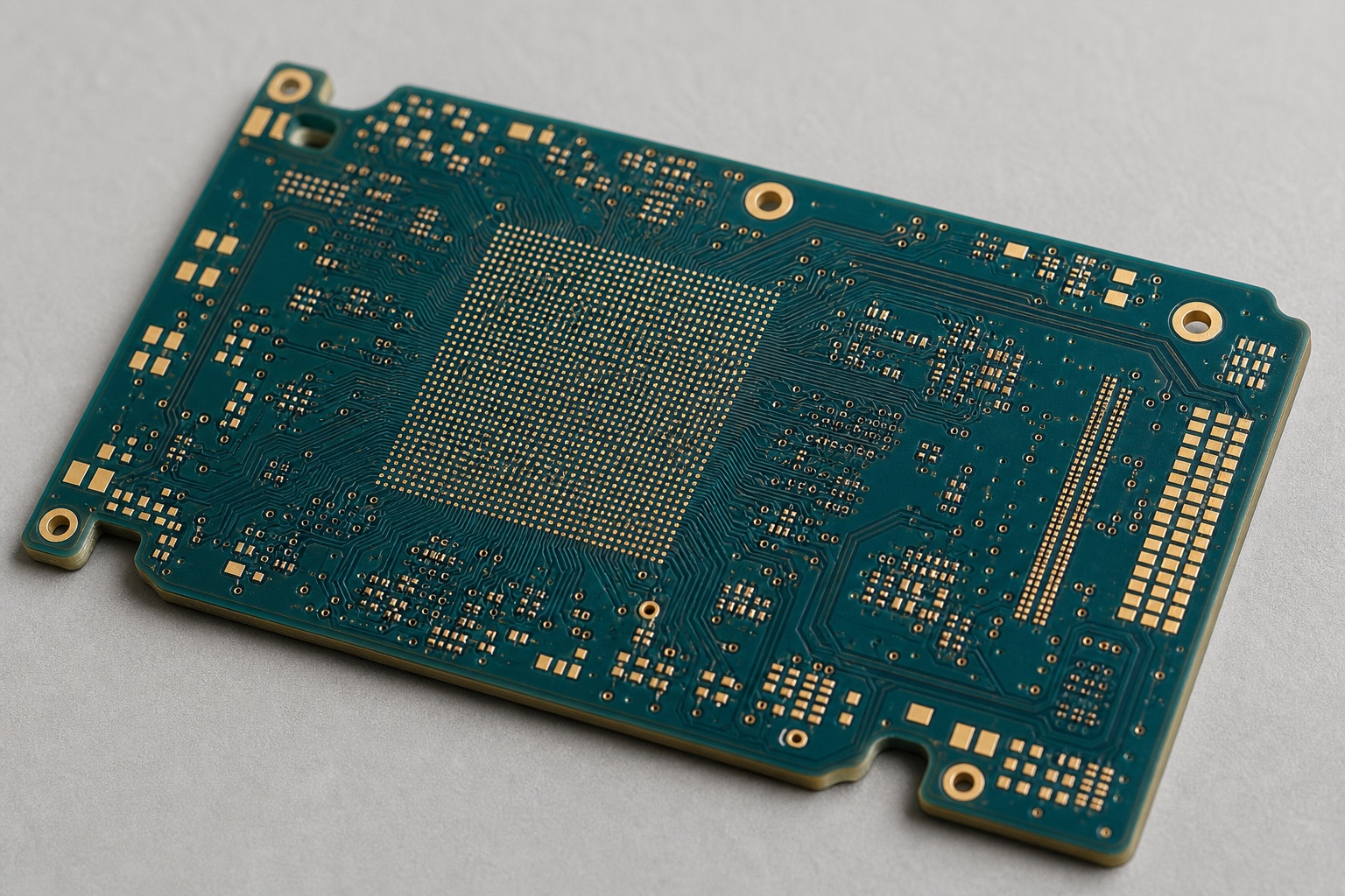
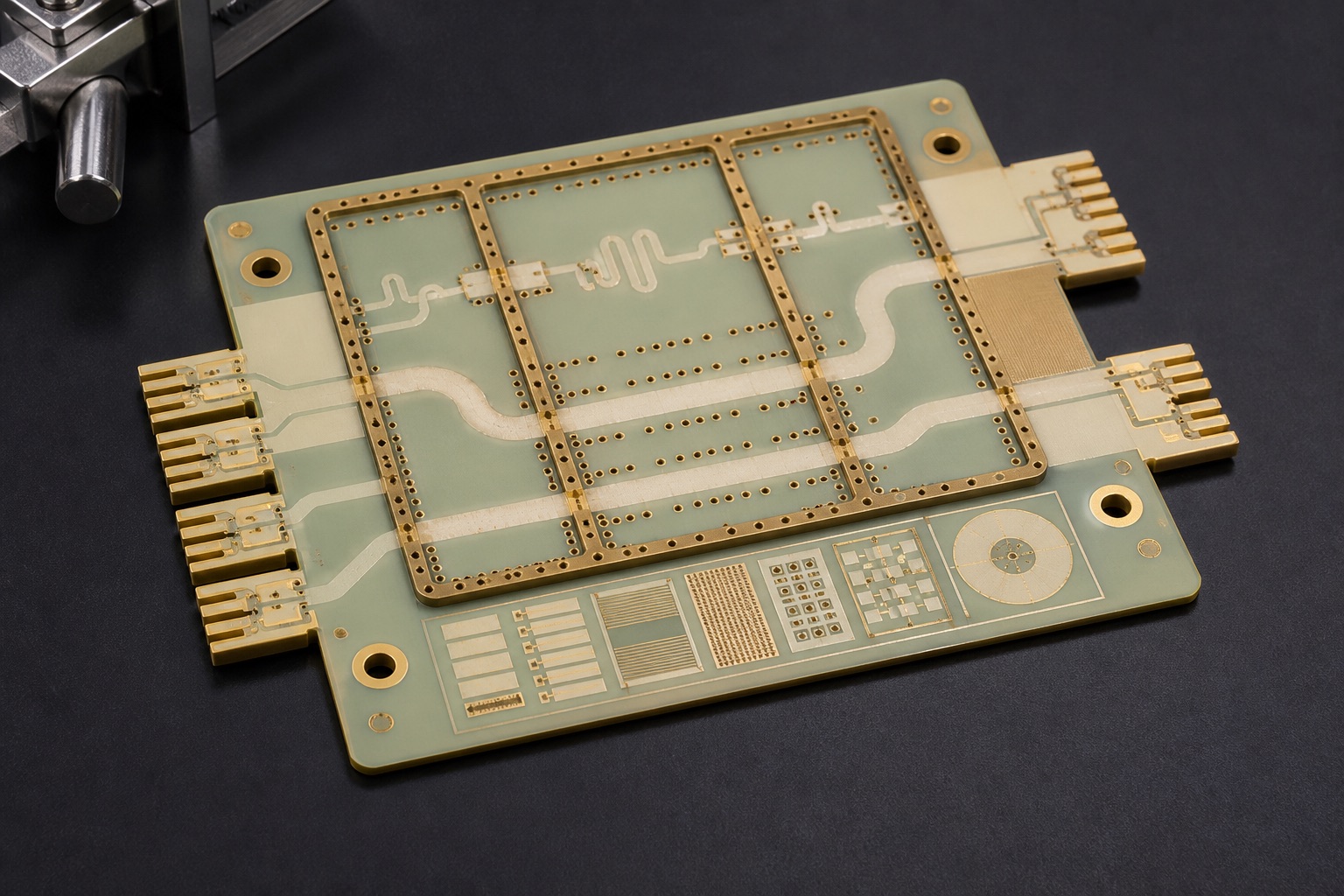
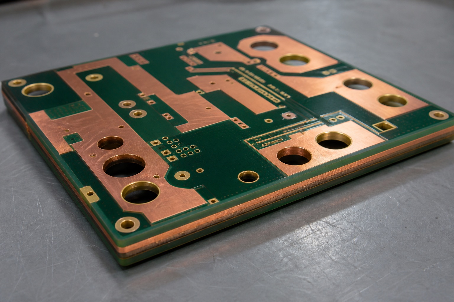
Representative visualization · not a customer board
Transparent status: These are representative engineering scenarios built from the capability boundaries published on this website. They are not anonymized customer case studies. A scenario becomes a production case study only after the actual project record, dates, quantity, results and publication permission are verified.
Representative visualization — not a customer board or factory photograph.
Scenario 01 · Controlled impedance
Mixed-material RF stack-up
A high-frequency design requires a manufacturable construction while preserving material intent, controlled impedance and critical transmission-line geometry.
Engineering review focuses on
Specified laminate grade and permitted alternatives
Reference layers, dielectric assumptions and copper profile
Single-ended or differential targets and tolerances
Critical line geometry, plating and surface finish
Coupon design and impedance measurement plan
Expected review outputEngineer-confirmed construction assumptions, DFM questions, impedance plan and quotation conditions.
Quantity
Defined per RFQ
Lead time
Confirmed after DFM, material and capacity review
Production result
Not claimed in this representative scenario
Representative visualization — not a customer board or factory photograph.
Scenario 02 · HDI / microvia
Fine-pitch module with microvias
A compact layout uses microvias or via-in-pad structures to escape a fine-pitch device while controlling registration, copper balance and fill requirements.
Engineering review focuses on
Blind and buried via transitions
Stacked or staggered microvia construction
Laser-via, capture-pad and target-pad geometry
Resin fill, capping and sequential lamination
AOI, microsection and electrical-test requirements
Expected review outputA feasible via and lamination route, identified design exceptions, inspection assumptions and commercial inputs. Actual capability is confirmed from the released data.
Quantity
Defined per RFQ
Lead time
Confirmed after DFM, material and capacity review
Production result
Not claimed in this representative scenario
Representative visualization — not a customer board or factory photograph.
Scenario 03 · Heavy copper
Power-control board with thick copper
A power design must balance current and thermal intent with etching limits, conductor clearance, hole-wall requirements and finished thickness.
Engineering review focuses on
Inner- and outer-layer copper requirement
Minimum conductor width and clearance
Copper distribution, thermal transitions and resin fill
Finished holes, annular rings and plating requirements
Surface finish, electrical test and microsection plan
Expected review outputDesign-rule exceptions, a proposed heavy-copper route, test assumptions and quotation scope.