PCB manufacturing · Guilin production base · Shenzhen service officesales@hxlfab.com

HDI and microvia fabrication

HDI PCB manufacturer

For compact hardware that needs finer routing and higher interconnect density, HXLFAB reviews microvia structure, sequential build requirements, via filling, capture pads and material selection before confirming the process route.

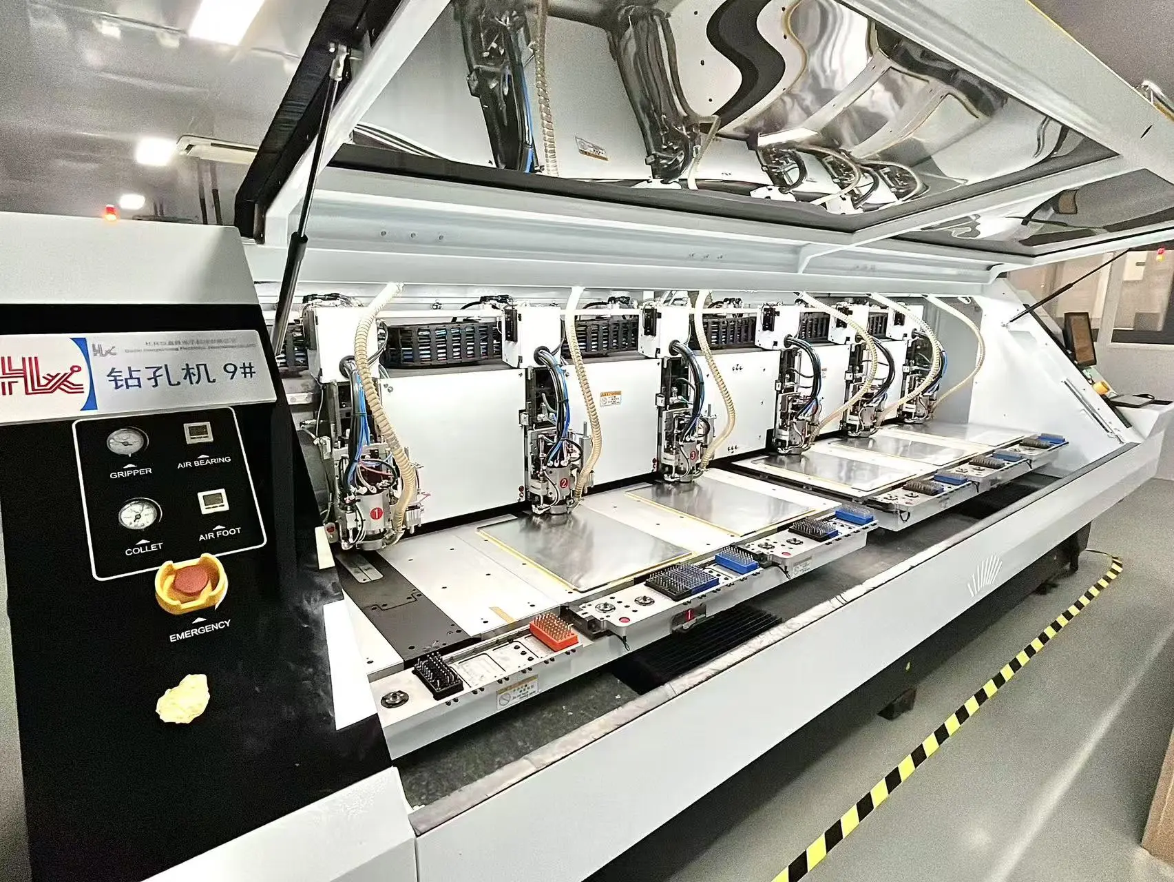
Multi-spindle precision drilling equipment at HXLFAB
Precision drilling and via preparation
0.10 mmMinimum laser via
3/3 milMinimum trace / space
Via-in-padAvailable by review
1–30Total layer capability

Engineering approach

Microvia structures reviewed as a complete build

HDI designs concentrate routing transitions into smaller spaces, which makes pad geometry, dielectric thickness, copper balance and lamination sequence especially important. A microvia that is feasible in isolation may still conflict with the complete stack-up.

HXLFAB evaluates blind and buried via intent, via-in-pad requirements, filling and capping, layer transitions and registration demands together. Final availability depends on the design data, material system and reliability requirements.

Engineering review includes

  • Laser-via diameter, capture pad and target pad geometry
  • Blind, buried and staggered microvia layer transitions
  • Via-in-pad filling and capping requirements
  • Sequential lamination and dielectric selection
  • Fine-line routing, copper balance and impedance interaction

Manufacturing envelope

Capabilities for quotation planning

These values describe the available manufacturing envelope. Final capability, lead time and price are confirmed after review of the actual production data, construction, material and quantity.

Minimum laser via0.10 mm subject to construction review
Trace / spaceDown to 3/3 mil subject to copper weight and design
Via structuresBlind, buried, staggered microvia and via-in-pad options by review
Via treatmentPlugging, resin filling and capping options according to the fabrication specification
MaterialsHigh-TG, halogen-free, CAF-resistant and application-specific systems
InspectionAOI, microsection analysis, electrical test and targeted process checks
Quote inputGerber/ODB++, stack-up, via table, impedance requirements and quantity

From RFQ to release

A controlled engineering workflow

01 / DATA REVIEW

Check the fabrication package

Gerber or ODB++, drill data, drawings, stack-up and requirements are checked for completeness.

02 / DFM & ROUTING

Confirm the process route

Engineering evaluates materials, features, via construction, test coverage and manufacturing risk.

03 / QUOTE & RELEASE

Issue confirmed terms

Price and lead time are confirmed after the technical route and commercial inputs are aligned.

Applications

Where this capability is used

Compact communications

Dense routing for radios, gateways and network modules.

Embedded compute

Fine-pitch packages and compact high-performance processors.

Medical electronics

Space-constrained diagnostic and monitoring hardware.

Automotive modules

Compact control and sensing electronics for qualified programs.

AI edge hardware

Dense interconnect for accelerators and edge computing.

Miniaturized devices

Products where board area and interconnect density drive the architecture.

Frequently asked questions

Before you request a quote

What is the minimum laser-via size?

HXLFAB lists 0.10 mm as the minimum laser-via capability. The finished construction, pad geometry, material and reliability requirements must be reviewed before confirmation.

Do you support via-in-pad?

Via-in-pad, resin filling and capping can be reviewed. Provide the via table and clearly identify filled, capped or plated-over requirements in the fabrication notes.

Can every blind-via design use the same process?

No. The lamination sequence depends on which layers are connected, whether vias are stacked or staggered, and the selected dielectric system.

What information speeds up an HDI quotation?

Provide complete production data, stack-up, via transition table, finished thickness, copper weights, impedance requirements, quantity and the component pad constraints that drive the HDI structure.

Ready to review your PCB build?

Upload Gerber files ↗