PCB manufacturing · Guilin production base · Shenzhen service officesales@hxlfab.com

Heavy-copper PCB fabrication

Heavy copper PCB manufacturer

Design and source thick-copper boards with conductor spacing, thermal distribution, plating, etching, finished thickness and mechanical limits reviewed as one manufacturing system.

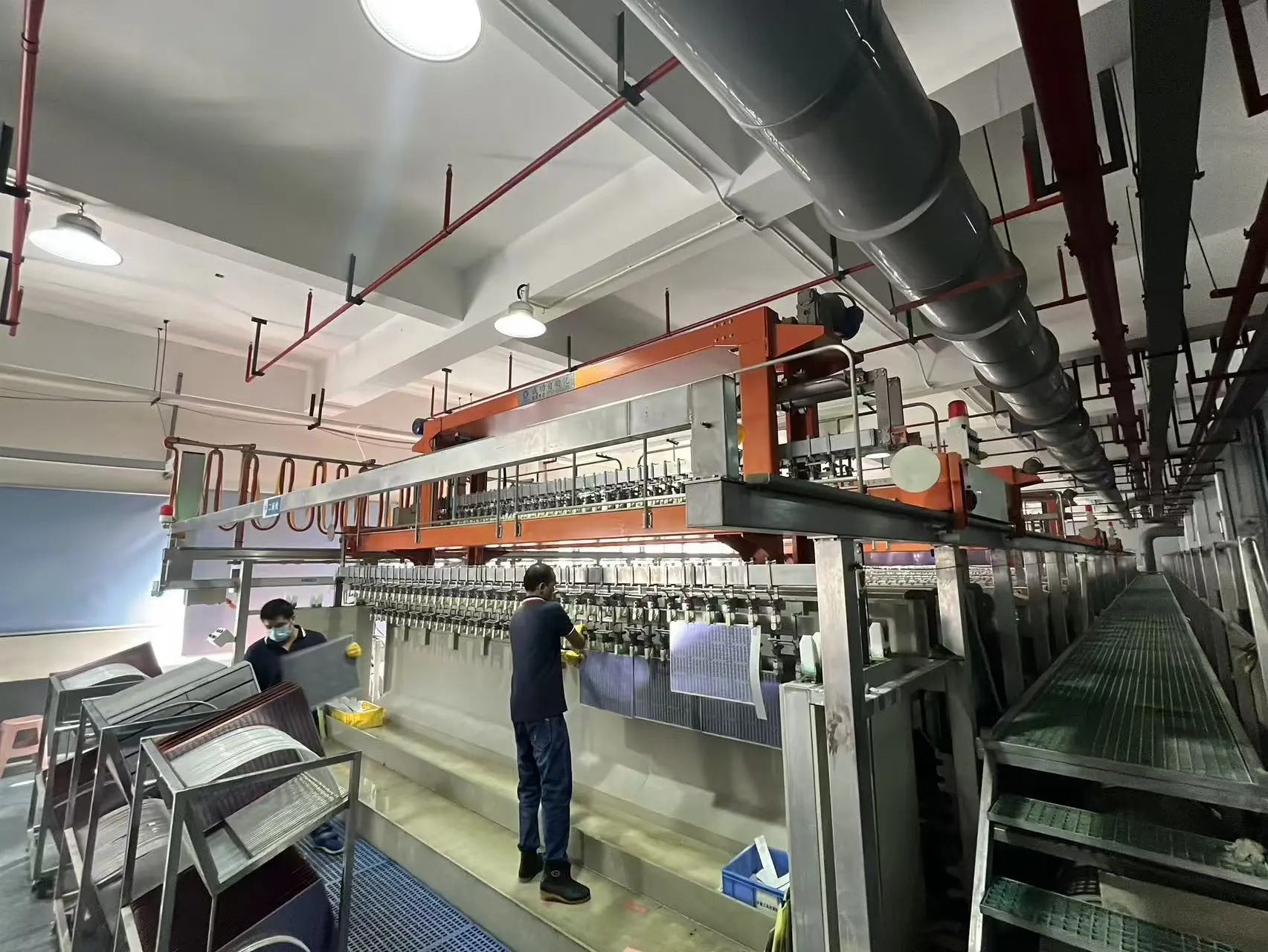
HXLFAB automated plating production line for PCB fabrication
Automated plating process control
4 ozInner-layer copper capability
8 ozOuter-layer copper capability
7.0 mmMaximum finished thickness
850 × 520 mmMaximum panel

Engineering approach

Copper weight changes the complete design rule set

Heavy copper supports current carrying, thermal spreading and mechanical robustness, but it also changes etching behavior, conductor spacing, hole-wall plating, dielectric fill and overall thickness. Standard one-ounce design rules should not be copied directly into a thick-copper build.

HXLFAB reviews copper distribution, minimum features, clearances, thermal transitions, via requirements and stack-up symmetry before confirming a heavy-copper production route.

Engineering inputs that matter

  • Copper weight by layer, not only a single overall value
  • Minimum conductor width, clearance and current requirement
  • Thermal distribution and copper-balance strategy
  • Finished thickness, hole sizes and plated-hole requirements
  • Surface finish, solder-mask clearance and assembly constraints

Manufacturing envelope

Capabilities for quotation planning

These values describe the available manufacturing envelope. Final capability, lead time and price are confirmed after review of the actual production data, construction, material and quantity.

Inner-layer copperUp to 4 oz capability, subject to design review
Outer-layer copperUp to 8 oz capability, subject to design review
Finished thickness0.15–7.0 mm overall capability; heavy-copper construction determines the practical range
Panel sizeUp to 850 × 520 mm
MaterialsHigh-TG and application-specific FR-4 systems according to thermal and reliability requirements
Design reviewSpacing, etch compensation, resin fill, copper balance, drill and plating requirements
VerificationElectrical test, inspection and microsection analysis according to the agreed control plan

From RFQ to release

A controlled engineering workflow

01 / DATA REVIEW

Check the fabrication package

Gerber or ODB++, drill data, drawings, stack-up and requirements are checked for completeness.

02 / DFM & ROUTING

Confirm the process route

Engineering evaluates materials, features, via construction, test coverage and manufacturing risk.

03 / QUOTE & RELEASE

Issue confirmed terms

Price and lead time are confirmed after the technical route and commercial inputs are aligned.

Applications

Where this capability is used

Power electronics

Power conversion, distribution and switching assemblies.

New energy

Energy storage, charging, inverter and monitoring equipment.

Industrial drives

Motor control, drives and high-current automation hardware.

Automotive power

Qualified power and control modules for automotive programs.

LED and lighting

Power delivery and thermal-management boards.

Protection systems

High-current protection, relay and control electronics.

Frequently asked questions

Before you request a quote

Does 8 oz apply to every layer?

No. HXLFAB lists up to 4 oz inner-layer and 8 oz outer-layer capability. The practical copper weight depends on the complete stack-up and design rules.

Can I use normal trace spacing on a heavy-copper board?

Do not assume so. Thicker copper generally requires different conductor and spacing rules, which should be confirmed from the actual layer copper and geometry.

What should a heavy-copper RFQ include?

Specify copper weight per layer, stack-up, current and thermal requirements, minimum conductor geometry, finished thickness, hole plating requirements, quantity and acceptance criteria.

How is heavy-copper quality checked?

The control plan can include CAM review, process inspection, electrical testing and microsection analysis. Exact acceptance criteria should be defined in the fabrication specification.

Ready to review your PCB build?

Upload Gerber files ↗